Fujitsu used a technical briefing this week to lay out the clearest picture yet of FUJITSU-MONAKA, the 2-nanometer Arm server processor it has been developing since its Fugaku supercomputer days. The chip packs 144 cores onto a core die built on a 2nm process, then stacks that die face-to-face on separate SRAM and I/O dies fabricated on a cheaper, more mature 5nm node. Two sockets combine for 288 cores per node. Fujitsu says shipments begin in 2027.
The disclosure, first detailed in Fujitsu’s own conference materials and then unpacked by outlets including Tom’s Hardware and Wccftech, matters for a reason that goes beyond one vendor’s roadmap slide. It is a working example of a strategy the whole chip industry has been circling for two years: put only the transistors that actually need the newest, most expensive node on that node, and push everything else – cache, I/O, memory controllers – onto older, cheaper silicon stacked underneath. If Fujitsu can ship that design in volume in 2027, it becomes a template that AMD, Intel, and the hyperscalers’ custom-silicon teams will all have to answer.
What Fujitsu actually confirmed about Monaka
Fujitsu’s own published materials, the ones the company hands out at conferences like ISC and Hot Chips, are specific about a handful of numbers and vague about almost everything else. The confirmed core spec is 144 cores per socket, scaling to 288 cores in a two-socket node. The core die uses a 2nm process. The SRAM and I/O dies sit on 5nm, which Fujitsu’s own slide deck describes bluntly as the better fit for I/O and SRAM work, since those blocks do not benefit much from bleeding-edge transistor density and cost far less to fabricate there.
The chip supports Arm’s Scalable Vector Extension 2 at 256-bit width, a step down from the 512-bit SVE Fujitsu used in the A64FX processor that powered the original Fugaku machine. That is not a regression so much as a rebalancing: memory bandwidth, not raw vector width, has become the harder constraint in AI and HPC workloads, and Fujitsu’s materials pair the narrower vectors with 12 channels of DDR5 and PCI Express 6.0 with CXL 3.0 support. Fujitsu describes the target workloads as AI and high-performance computing, and the company’s own volume-shipment date is 2027.
Everything past that point, including the specific clock speeds and TDP figures now circulating in trade press, comes from journalists who attended Fujitsu’s Hot Chips 2026 session rather than from a formal product data sheet. That distinction matters for how the numbers should be read, and it is worth keeping in mind through the rest of this piece: where a figure is described as reported rather than confirmed, it has not appeared in Fujitsu’s own published documentation surfaced so far.
The 3D chiplet trick: why split 2nm from 5nm at all
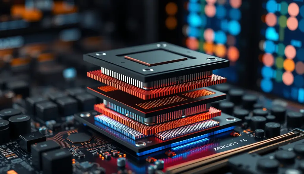
The headline engineering decision in Monaka is disaggregation by cost, not just by function. A modern 2nm wafer from TSMC costs dramatically more per square millimeter than a 5nm wafer. Cache and I/O logic are large, low-transistor-density structures – building them on the newest node wastes expensive area on circuits that do not run any faster for it. Fujitsu’s answer is to build only the compute cores on 2nm, then bond a separate SRAM die and a separate I/O die, both on 5nm, directly underneath using face-to-face hybrid copper bonding.
Reports from the Hot Chips 2026 session, including coverage from ServeTheHome, describe the last-level cache being moved onto its own separate 5nm die entirely, stacked beneath the compute tile. That is a more aggressive split than most chiplet designs attempt today, where cache typically still lives on the same die as the cores. The approach echoes what The Register has reported about Fujitsu’s packaging partnership with Broadcom for the 3D stacking work, since hybrid bonding at this scale requires packaging expertise that few foundries have industrialized.
Fujitsu’s own materials put a number on the payoff: stacking the 2nm core die on top of 5nm SRAM cuts total silicon area by roughly 30% compared with building everything on the leading node. That is a direct cost lever, not just an efficiency claim, and it explains why a company the size of Fujitsu – nowhere near Nvidia or AMD’s chip design budgets – believes it can compete on a 2nm data-center part at all. It is buying less 2nm silicon per chip than a monolithic design would need.
Monaka specs at a glance
| Spec | FUJITSU-MONAKA | Source status |
|---|---|---|
| Core count | 144 cores per socket, 288 per 2-socket node | Fujitsu official |
| Core die process | 2nm | Fujitsu official |
| SRAM / I/O die process | 5nm | Fujitsu official |
| Vector extension | Arm SVE2, 256-bit | Fujitsu official |
| Memory | DDR5, 12 channels | Fujitsu official |
| Interconnect | PCIe 6.0, CXL 3.0 | Fujitsu official |
| Target workloads | AI and HPC | Fujitsu official |
| Shipments | 2027 | Fujitsu official |
| Air-cooled SKU clocks/TDP | Reported around 2.1GHz base, 350W | Reported by trade press |
| Liquid-cooled SKU clocks/TDP | Reported around 2.9GHz base, 500W | Reported by trade press |
Monaka-X: what’s confirmed, what’s still a rumor
The most attention-grabbing part of this story is also the least confirmed. Wccftech’s report frames a follow-on chip called Monaka-X as targeting a 1.4nm process, a 2029 release window, and support for Nvidia’s NVLink Fusion interconnect, which would let a Fujitsu Arm CPU talk to Nvidia GPUs at the same coherent-memory speeds Nvidia’s own Grace CPU enjoys today. None of those three claims – 1.4nm, 2029, or NVLink Fusion – appear in the Fujitsu source documents surfaced during this reporting cycle. They are being reported by outlets covering the Hot Chips and industry-roadmap circuit, not stated in Fujitsu’s own published slide decks.
That gap between “what a company presented” and “what a company is quietly telling briefed journalists” is normal in chip roadmaps this far out, and it is not automatically a reason for skepticism. Fujitsu has form here: the company committed to Monaka’s core architecture years before this month’s public data dump, and it has run a fairly disciplined public roadmap process tied to Japan’s national supercomputing program since the K computer era. But readers evaluating whether to plan hardware or software strategy around Monaka-X specifically should treat every number attached to that name as provisional until Fujitsu confirms it directly, the same caution any hardware buyer would apply to an unreleased product three years out.
If NVLink Fusion support does materialize on Monaka-X, it would be notable mainly because Nvidia opened that interconnect to third-party CPU vendors specifically to avoid ceding the AI server market to Arm-only or x86-only stacks. A Fujitsu CPU wired into Nvidia’s coherent-memory fabric would put Fujitsu in the same conversation as Nvidia’s own Grace CPU and MediaTek’s Arm designs for Nvidia’s next-generation racks – a meaningfully different market position than Fujitsu occupies today, where Monaka is mostly discussed in the context of Japan’s domestic HPC procurement.
How Monaka compares with the field
Fujitsu is not the only company chasing disaggregated, multi-node designs for AI and HPC. AMD’s Epyc “Turin” and upcoming “Venice” generations already split I/O dies from compute dies on mature nodes, though AMD keeps cache on the compute chiplet rather than moving it to its own separate tier. Intel’s Xeon roadmap has leaned on tile-based designs since Sapphire Rapids, again without the aggressive face-to-face SRAM stacking Fujitsu is describing. Nvidia’s Grace CPU, meanwhile, is an Arm design built specifically to pair with Nvidia GPUs over NVLink-C2C, which is precisely the lane Monaka-X is rumored to be trying to enter from the outside.
What sets Monaka apart on paper is the specific decision to move the entire last-level cache off the compute die and onto its own 5nm tile. Most competing designs still keep at least some cache on the same silicon as the cores, accepting the node-cost penalty in exchange for lower interconnect latency between cores and cache. Fujitsu is betting that hybrid copper bonding is now mature enough to make that latency penalty small, a bet that will be tested once independent benchmarks of shipping silicon exist rather than vendor projections.
Competitive positioning table
| Processor | Architecture | Node strategy | Target ship |
|---|---|---|---|
| Fujitsu Monaka | Arm SVE2, 144 cores/socket | 2nm core die + 5nm SRAM/I/O, 3D-stacked | 2027 |
| Nvidia Grace | Arm, Nvidia-designed cores | Monolithic on TSMC leading node | Shipping |
| AMD Epyc (current gen) | x86, chiplet | Compute chiplets on leading node, I/O die on mature node | Shipping |
| Intel Xeon (tile-based) | x86, tile-based | Multiple tiles, mixed nodes | Shipping |
| Fujitsu Monaka-X (reported) | Arm, next-gen | Reported 1.4nm, NVLink Fusion | Reported 2029, unconfirmed by Fujitsu |
Historical context: from the K computer to Fugaku to Monaka
Fujitsu did not arrive at a 2nm Arm server chip by accident. The company built the CPU for the K computer, which topped the TOP500 supercomputer ranking in 2011, and later designed the A64FX processor that powered Fugaku, the machine that held the world’s top HPC ranking for multiple cycles starting in 2020. A64FX was itself notable for using 512-bit SVE vectors on Armv8-A, a choice that made Fugaku unusually strong on vectorized scientific workloads.
Monaka represents a generational shift in that lineage on two fronts. It moves from Armv8-A to Armv9-A, and it narrows vector width from 512-bit to 256-bit SVE2 while leaning harder on core count, memory bandwidth, and 3D packaging to make up the difference. That is consistent with an industry-wide trend: raw vector width matters less than it did a decade ago, because modern AI and HPC codebases increasingly bottleneck on memory bandwidth and interconnect rather than pure FLOPs per core. Fujitsu’s pivot to a chiplet architecture with 12-channel DDR5 and CXL 3.0 support reads as a direct response to that shift.
It also positions Fujitsu as one of the few non-American, non-Chinese companies attempting to design a leading-edge server CPU from scratch rather than licensing a reference design. That matters to Japan’s broader push for what Fujitsu’s own materials describe as sovereign AI and HPC infrastructure: a domestically designed processor gives Japan’s government and research institutions a supply chain that does not run entirely through Nvidia, AMD, or Intel roadmaps.
Why the 5nm SRAM decision is the real story
It is tempting to read “2nm CPU” as the headline and move on, but the more consequential decision in Monaka’s design is arguably the one buried in Fujitsu’s own slide: putting SRAM and I/O on 5nm specifically because that node is a better economic and electrical fit for those blocks. SRAM density scaling has slowed sharply on the newest nodes – moving from 5nm to 2nm barely shrinks SRAM cells anymore, even though it shrinks logic transistors substantially. That means paying 2nm prices for SRAM buys almost nothing in return.
Chip designers across the industry have quietly reached the same conclusion over the past two years, which is why Monaka’s approach is being watched as a bellwether rather than a curiosity. If Fujitsu’s 30% area reduction claim holds up once independent teardown analysis is possible, expect AMD, Intel, and custom-silicon teams at Amazon, Google, and Microsoft to lean further into the same split-node, stacked-SRAM approach for their own next-generation server and AI accelerator designs.
Market impact: what this means for the AI infrastructure race
For hyperscalers and HPC operators shopping for 2027-era infrastructure, Monaka adds a fourth serious option to a field that has effectively been a three-way race between Nvidia’s Grace, AMD’s Epyc line, and Intel’s Xeon roadmap. Fujitsu is not going to out-ship any of those three in raw unit volume, but it does not need to in order to matter. Japan’s national research institutions, and any customer prioritizing a non-US, non-Chinese supply chain for sovereign AI infrastructure, now have a credible domestically designed alternative with a committed 2027 shipment date.
The AI and HPC framing in Fujitsu’s own materials is deliberate. A pure HPC chip with no AI story would struggle to justify the R&D spend a 2nm design requires, since HPC procurement cycles are slower and smaller than AI infrastructure spending. By explicitly targeting both markets and building in PCIe 6.0 and CXL 3.0 support for tighter coupling with AI accelerators, Fujitsu is positioning Monaka to ride the same capital wave that has been funding Nvidia, AMD, and the hyperscalers’ custom silicon efforts rather than competing only for the shrinking pool of pure supercomputing budgets.
There is also a packaging supply-chain angle worth watching. Face-to-face hybrid copper bonding at this scale depends on advanced packaging capacity that is already tight because Nvidia, AMD, and others are competing for the same CoWoS and bonding lines at TSMC and its partners, a crunch SDxCentral has covered in the context of Broadcom’s own push into 2nm AI chip packaging. Fujitsu securing packaging capacity for a 2027 volume ramp is itself a signal that the company has locked in supply agreements well ahead of launch, something smaller HPC vendors have struggled to do in a market where Nvidia’s GPU demand has strained advanced packaging capacity for several years running.
What developers and infrastructure teams should watch for
Software teams evaluating Arm server platforms should treat Monaka the way they treated Grace and Ampere Altra before it: as a strong reason to make sure build pipelines, container images, and dependency chains are Arm-clean well before hardware ships. The move to Armv9-A with 256-bit SVE2 means code tuned specifically for A64FX’s 512-bit SVE will need re-tuning rather than a straight recompile, particularly for HPC codebases that hand-vectorized around the wider register width.
Teams planning AI training or inference infrastructure around a 2027 timeline should also watch the CXL 3.0 and PCIe 6.0 support closely. Those two standards are still maturing across the accelerator ecosystem, and a CPU that ships production-ready CXL 3.0 support in 2027 will only be as useful as the memory-expansion and accelerator hardware available to pair with it at that point. Fujitsu shipping the CPU side of that equation on schedule does not guarantee the rest of the ecosystem, GPUs, memory expanders, interconnect switches, will be equally ready.
Predictions: where this goes from here
- Expect Fujitsu to publish more granular official performance figures (clock speeds, TDP, and benchmark numbers) closer to its 2027 shipment date, since the specific figures now circulating are attributed to trade press coverage of the Hot Chips session rather than a formal Fujitsu data sheet.
- Expect AMD, Intel, and at least one hyperscaler custom-silicon team to publicly discuss or demonstrate a similar split-node, stacked-SRAM chiplet approach within the next 12 to 18 months, following the same cost logic Fujitsu’s materials lay out.
- Expect continued ambiguity around Monaka-X’s 1.4nm target and 2029 timeline until Fujitsu issues its own roadmap update, given that neither figure currently appears in the company’s published documentation.
- Expect Japan’s national research and government procurement programs to be the first confirmed Monaka customers, ahead of any broader commercial hyperscaler adoption, consistent with the sovereign-AI framing in Fujitsu’s own materials.
- If NVLink Fusion support is eventually confirmed for Monaka-X, expect Nvidia to promote the partnership publicly as evidence that its coherent-interconnect strategy is gaining traction beyond its own Grace CPU line.
The bigger picture: node economics are reshaping chip design
Monaka is a useful case study in a broader shift happening across the chip industry: the leading process node is no longer treated as a blanket upgrade applied to an entire chip. It is increasingly treated as a scarce, expensive resource reserved for the specific transistors that benefit most from it, with everything else pushed onto cheaper, more mature silicon and stitched back together through advanced packaging. That is the same logic behind chiplet designs from AMD and Intel, and it is the same logic Apple and Nvidia apply when deciding which parts of a system-on-chip get the newest node and which do not.
What makes Fujitsu’s version notable is how far it pushes the split: not just I/O onto a separate die, which is now common, but the entire last-level cache onto its own 5nm tile, bonded face-to-face beneath the compute die. If that design ships on schedule in 2027 and performs as advertised, it will be one of the most aggressive examples yet of treating a leading node as a scalpel rather than a blanket, and it will give every other chip designer a concrete data point on whether that bet pays off.
FAQ: Fujitsu Monaka and Monaka-X
What is FUJITSU-MONAKA?
FUJITSU-MONAKA is Fujitsu’s next-generation Arm-based server processor, built with a 2nm core die stacked on 5nm SRAM and I/O dies. It packs 144 cores per socket, scaling to 288 cores across two sockets, and Fujitsu has said shipments begin in 2027.
Is Monaka a 2nm chip or a 5nm chip?
Both, by design. The core compute die uses a 2nm process, while the separate SRAM and I/O dies stacked beneath it use a 5nm process, since Fujitsu’s own materials describe 5nm as the better fit for those specific blocks.
How many cores does Monaka have?
144 cores per socket. In a two-socket server configuration, that scales to 288 cores per node, according to Fujitsu’s official materials.
What is Monaka-X and is it confirmed?
Monaka-X is a reported follow-on chip that trade press, including Wccftech, describes as targeting a 1.4nm process, a 2029 release, and support for Nvidia’s NVLink Fusion interconnect. None of those three specific details have appeared in Fujitsu’s own published materials surfaced so far, so they should be treated as reported rather than confirmed.
When will Monaka ship?
Fujitsu’s official materials state that product shipments begin in 2027.
What vector extension does Monaka use?
Monaka supports Arm’s Scalable Vector Extension 2 (SVE2) at 256-bit width, narrower than the 512-bit SVE used in Fujitsu’s earlier A64FX processor.
How does Monaka compare to Nvidia’s Grace CPU?
Both are Arm-based server processors, but Grace is designed by Nvidia specifically to pair with Nvidia GPUs over its NVLink-C2C interconnect and is already shipping. Monaka is Fujitsu’s independently designed processor built around a more aggressive 3D chiplet split between 2nm and 5nm dies, with shipments targeted for 2027.
Why does the SRAM process node matter?
SRAM density barely improves on the newest process nodes, so building SRAM on a cheaper, more mature node like 5nm instead of 2nm saves cost without sacrificing much density. Fujitsu’s materials say this approach cuts total silicon area by roughly 30% compared with a monolithic 2nm design.
- HBM4 Memory Hits 80% Yield, Powers Nvidia Rubin
- HPE Stock Hits 52-Week High of $58.79 on Nvidia CPU
- Nvidia Reportedly Buys Hugging Face for $12.9B
- AWS-NVIDIA Deal Adds 2M GPUs as AWS Buys DuckDB
- Jalapeño Chip: OpenAI Targets Nvidia’s 75% Margin
- More Hardware & Chips Coverage